PCBA Appearance Inspection Standard
1. Objective
Establish PCBA appearance inspection standards to provide guidance for the operation of the production process and product quality assurance to ensure that the product quality meets the needs of customers.
2. Scope of Application
2.1 This standard shall be used for the appearance inspection of PCBA of all products produced by the company (except for the cases without special regulations), including products produced within the company or processed outside the company.
2.2 Special provisions shall mean that the PCBA standards may be modified as appropriate due to the characteristics of the parts or other special requirements, and their effectiveness shall exceed the general appearance standards.
3. Precautions for standard use:
3.1 "Unqualified" refers to the product meets the unqualified judgment specified in the standard.
3.2 Requirements for appearance inspection items of IPQC or FQC are respectively specified in the judgment.
3.3 If the product does not meet the criteria of the unqualified judgment, it shall be regarded as qualified product;
3.4 If the product meets the criteria of unqualified judgment, it shall be regarded as unqualified product, and it shall be dealt with according to the treatment method of unqualified product.
3.5 Schematic drawings are for reference only, and it is not required for parts with drawings.
3.6 If there is no schematic diagram for some product parts, you can refer to the schematic diagram of other categories.
3.7 The maximum size refers to those measured in all directions.
3.8 When filling in the quality report of each process, the defect item list indicated in this document shall be selected as the basis for recording corresponding defect. If there is a defect that is not indicated in the defect item list, the defect name shall be filled in the remark column below the quality report.
4. Identification and handling methods for unqualified products:
4.1 Mark the defective parts of the unqualified products (with small red arrow) and record them in the corresponding defect column on the inspection report. The unqualified products should be separated from the qualified products to avoid confusion.
4.2 All unqualified products must be returned to the corresponding production process for repair (or rework). For special cases of machine boards, such as copper peeling, PCB green oil coming off, green oil blistering, PCB oil replenishing, etc., they should be classified according to actual situation and handled separately.
5. Criteria definition
5.1 Criteria
5.1.1 Acceptance criteria: acceptance criteria are target condition, accept condition and reject condition.
5.1.2 Target condition: if the assembly condition is not in line with the target or perfect assembly condition but has good assembly reliability, it can be judged as target condition.
5.1.3 Accept condition: if the assembly condition is not in conformity with but is close to the target condition, it can be judged as accept condition.
5.1.4 Reject condition: if the assembly condition does not meet the acceptance criteria, which may affect the functionality of the product, it can be judged as reject condition in order to maintain the competitiveness of the company's products.
5.1.5 The priority of engineering documents, production process documents and quality work guidelines: when the contents of the appearance accept condition conflict with those of engineering documents, production process documents and quality work guidelines, the contents of other instructions listed are preferred. Other special requirements not listed in the appearance acceptance criteria may be referred to quality work guidelines or other process documents.
5.2 Defects definition
5.2.1 Critical defect: it refers to a defect that is sufficient to cause harm to the human body or machinery, or threaten life or property, which is expressed by CR.
5.2.2 Major defect: it refers to a defect that reduces the practicability or reliability of a product, causing product damage and dysfunction, which is expressed by MA.
5.2.3 Minor defect: it refers to a defect in appearance or mechanism assembly, which does not affect the practicability or the performance of a product, expressed by MI.
6. Reference documents
Refer to IPC-A-610 inspection standard Acceptability of Electronic Assemblies.
7. Pre-inspection preparation:
7.1 Inspection conditions: more than 500 LUX of indoor lighting;
7.2 Inspection tools: 10x illuminating magnifying glass, 40x microscope;
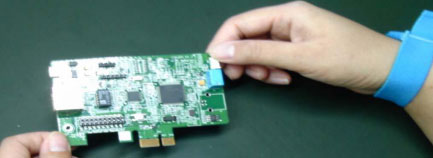
7.3 ESD protection: Any contact with PCBA semi-finished products must be equipped with electrostatic protection measures (anti-static wristband connected to an electrostatic grounding wire or anti-static gloves).
7.4 Before the inspection, it is necessary to confirm that the working platform used is clean and the gloves worn are clean anti-static gloves.
8. Description and schematic diagram of unqualified items: see attached page for details
8.1 PCBA holding mode
8.1.1 Target condition
(1) Wear clean anti-static gloves and take electrostatic protection measures;
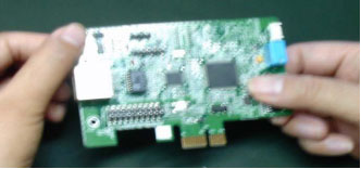
(2) Hold the edge or corner of the board for inspection;

8.1.2 Accept condition
Hold the edges or corners of the PCB for inspection with electrostatic protection measures.

8.1.3 Reject condition
Contact with the surface of the conductor and the tin point directly without electrostatic protection measures.

9. Explanation and definition of soldering terms
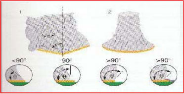
(1) Wetting: a solder coating is formed on the surface. The smaller the wetting angle, the better the wetting ability.
(2) Wetting angle: the angle enclosed by the wiring between the solid metal surface and the molten solder (as shown in the figure below). Generally, it is the interface between the liquid surface and other soldered bodies or liquids. The smaller the angle, the better the solder ability.
(3) Non-wetting: no solder-like coating is formed on the surface, and the wetting angle is greater than 90 degrees in this case.
(4) De-wetting: when the original solder is retracted, a very thin solder film will be left. As the solder retracts, the wetting angle increases.
(5) Solderability: the surface characteristic that is easily stained by molten solder.

10. Process standard for ideal solder joints
(1) The solder joint on the solder side of the board shall be a solid cone with flat top; the two outer edges of the cross-sectional view shall present a uniform arc of crescent column, and the through hole shall be filled with solder to evenly and completely wrap the foot of the part.
(2) The bottom area of the cone should be consistent with the land, pad and annular ring on the board.
(3) The climbing height of the flat-topped cone is about three-quarters of the part feet protruding from the circuit board; the maximum height should not exceed one-half or 80% of the diameter of the solder pad (otherwise it is easy to cause a short circuit).
(4) It is better to fill the edge of the pad and the foot of the part, and the wetting angle should be close to zero. The better the wetting angle, the better the solder ability.
(5) The solder side shall be glossy (it should not affected by other factors, such as being exposed to chemicals, which will tarnish the surface): the surface shall be smooth and free from any irregularities, such as small chips, blisters and inclusions.
(6) For boards plated with through holes, the solder should climb into the hole from the solder surface and rise to the component side. The solder on the solder surface should be smooth and meet the requirements of Point 1 to Point 5.
11. General requirement criteria: soldering technical standards
11.1 Good solder ability are defined as follows:
11.11 Wetting angle is lower than 90 degrees;
11.12 There are no bad conditions such as de-wetting and non-wetting;
11.13 Wetting is distinguishable on the solder side.
11.2 Solder balls: the following two conditions are acceptable, and the others are unqualified.
11.21 Unremovable solder balls with a diameter less than 0.25 mm (on the solder side);
11.22 Solder balls with a diameter less than 0.13mm on the surface of the part, which neither stick on the foot of the part nor cause short circuit.
11.3 Excess solder: the following conditions are acceptable, and the rest are unqualified.
11.31 The solder side is convex, but there is no non-wetting or de-wetting;
11.32 Solder does not extend to PCB or parts;
11.33 The part foot should be seen protrude out of the solder side (in accordance with the part foot length criteria);
11.34 No tin dross by visual inspection is acceptable;
11.35 Meets criteria of solder icicles or solder balls on the working hole.
Excess solder rejection criteria:
1. The solder extends to the body of the part;
2. Part foot does not protrude out of the solder side by visual inspection;
3. The solder extends beyond the solder pad and touches the board.
11.4 Part foot length criteria
11.41 The part foot must protrude out of the tin surface (the part foot can be seen to be exposed by visual inspection).
11.42 The protruding length of the foot of the part is greater than 0.2mm and less than 2mm.
11.5 Cold welding/ bad solder joint
11.51 No cold welding or bad solder joint is allowed.
11.52 Solder joints shall be free of unfused solder paste.
11.6 Solder crack
No solder crack is allowed.
11.7 Solder icicles
No solder icicle is allowed (if the solder icicle is too long, it will easily penetrate the insulating sheet and cause grounding with the iron shell, which will damage the motherboard).
11 .8 Pin hole
11.81 Visually visible pin holes are not accepted.
11.82 Pin holes should not penetrate vias.
11.83 There should be no defects such as de-wetting and non-wetting.
11.9 Broken holes/ blow holes
There must be no broken holes/ blow holes.
11.10 Solder bridge (short circuit)
There must be no solder bridge, which will cause a short circuit when two conductors are bridged.
11.11 Solder dross
Visually visible solder dross is not accepted.
11.12 Excess solder in the assembly screw hole
The height of solder balls and solder icicles on the assembly screw hole on the surface of the part shall not be greater than 0.6 mm.
11.12.2 Excess solder in the assembly screw hole on the solder side is not allowed.
11.12.3 The inner hole wall of the screw hole shall not be stained with solder.
12. General criteria: PCB/parts criteria
12.1 PCB/part damage: slight damage:
12.1.1 Acceptable minor damage
● There are scratches on the body of plastic or ceramic parts, but the internal components of the parts are not exposed.
● There are slight scratches on the part body that will not damage the packaging of the parts or cause the parts to be unclearly marked.
12.2 PCB cleanliness
12.2.1 There should be no contaminants such as left over parts, (obvious) fingerprints, and dirt (dust).
12.2.2 Part materials such as thermal paste and circuit adhesives will not be accepted if they are offset.
12.2.3 Flux residues (such as water lines) can be accepted; white residues with a thin layer of residues (such as water lines) can be accepted, but powdery, granular and crystalline residues can not be accepted.
12.2.4 Visible solder dross will not be accepted when using 3 times or less magnifying glass (including visual inspection).
12.2.5 Loose metal burrs on the parts feet are not allowed.
12.3 PCB delamination/blistering is not acceptable.
12.4 Gold Finger criteria
12.4.1 The Gold Finger shall not be lifted or damaged. Its non-main (non-functional) contact area can be defective, but there should not be blisters;
12.4.2 Important parts of the Gold Finger must not be stained with any type of solder containing solder balls, tin dross, stains, etc.;
12.4.3 Other small flaws in the Gold Finger contact area, any size exceeding 0.25mm will not be accepted;
12.4.4 Accept criteria for soldering on Gold Finger:
The diameter of each point is not more than 0.3mm; no more than one point on each finger; no more than 3 points on each side.
12.4.5 Accept criteria for Gold Finger scratch
Scratches without exposed copper are acceptable. There shall be only one scratch in the whole row of fingers, and the depth and length of the notch shall be less than 0.07mm and 0.3mm respectively.
12.5 Bending:
PCB board bending or warping shall not exceed the thickness of 1 PCB.
12.6 Scratches:
12.6.1 Scratches as deep as the PCB fiber layer cannot be accepted.
12.6.2 Scratches as deep as the exposed copper of the PCB circuit is not accepted.
12.6.3 Line repair and green oil should not be too thick. The color difference should not be too obvious. There should be no exposed copper.
13. Other criteria
13.1 Polarity
Polarized parts must be placed in the correct position according to the instructions or PCB markings. The first piece of each batch must be made to find out whether there is any difference in the location of the parts and the actual content of the parts.
13.2 Sampling inspection
(1) Refer to AQL International Inspection Standard II, CR=0 MAJ=0.4 MIN=0.65. (See attached page for AQL sampling standards)
(2) Full inspection is adopted if the quantity is 100PCS or below.